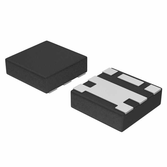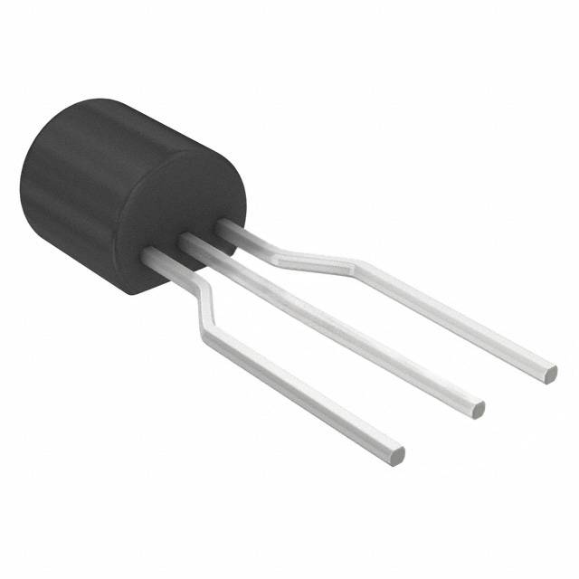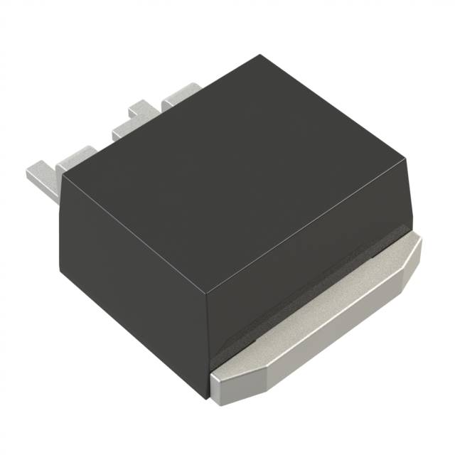
NTLUS3A90PZTBGP-Channel 20 V 2.6A (Ta) 600mW (Ta) Surface Mount 6-UDFN (1.6x1.6)
N/A
Orders Over $2000 Receive a $100 Discount for Registered Abrmicro Users.
ABRmicro #.ABR2045-NTLUS3-920798
ManufacturerOnsemi
MPN #.NTLUS3A90PZTBG
Estimated Lead Time-
SampleGet Free Sample
Datasheet NTLUS3A90PZ(PDF)
 NTLUS3A90PZ(PDF)
For large-volume purchases, our unique channels enable us to provide prices that other suppliers cannot match: significantly below market rates.
Service
 Guaranteed Authenticity
 Technical Support
 Fast Refund
 Free Shipping (over $960)
 Issue an Invoice
 24/7 Manual Service
 Technical Specifications
Series-
Packaging
Tape & Reel (TR)
Lifecycle StatusObsolete
Base Product NumberNTLUS3
Continuous Drain Current (ID) @ 25°C2.6A (Ta)
Drain-to-Source Voltage (VDS)20 V
Drain-to-Source On Resistance (Max. Min.Rᴅs(on))1.5V, 4.5V
FET Feature-
FET TypeP-Channel
Gate Charge Total (Qg)(Max.)12.3 nC @ 4.5 V
Common Source Input Capacitance (Cɪss)(Max.)@(Vᴅs)950 pF @ 10 V
Mfronsemi
Mounting StyleSurface Mount
Operating Temperature-55°C ~ 150°C (TJ)
Maximum Power Dissipation600mW (Ta)
RDS(on) Drain-to-Source On Resistance62mOhm @ 4A, 4.5V
Package Type (Mfr.)6-UDFN (1.6x1.6)
TechnologyMOSFET (Metal Oxide)
Gate-to-Source Voltage (Vɢs)±8V
VGS(th) Gate-to-Source Threshold Voltage (Max.)1V @ 250µA
Package / Case6-PowerUFDFN
Customize Part Specifications , or Contact Our Sales Representative to Obtain the Data You Desire info@Abrmicro.com
 info@Abrmicro.com
Extended Links
Datasheets
Environmental Information
PCN Design/Specification
PCN Obsolescence/ EOL
Environmental & Export Classifications
RoHS ComplianceComplies with RoHS 3 Directive (2015/863/EU)
MSL Level1 (Unlimited, ≤ 30°C/85% RH), No special packaging
REACH RegulationNo SVHCs Present
US ECCNEAR99
HTSUS8541.21.0095 (Other; No import duty applies)
Additional Details
The NTLUS3A90PZTBG is a P-Channel MOSFET produced by Onsemi, specifically designed for surface mount applications in a compact 6-UDFN package measuring 1.6x1.6 mm. It operates efficiently with a drain-source voltage rating of 20 V and a continuous drain current of 2.6A at thermal conditions defined by (Ta). The device can handle power dissipation of up to 600mW at ambient temperature. Additionally, the MOSFET features an input capacitance of 950 pF when subjected to a 10 V gate-source voltage, and it has a gate-source voltage rating of ±8 V, offering reliable performance for various electronic applications requiring compact and efficient components.
This information is sourced from the Internet, hasn't been reviewed, and may contain errors.


