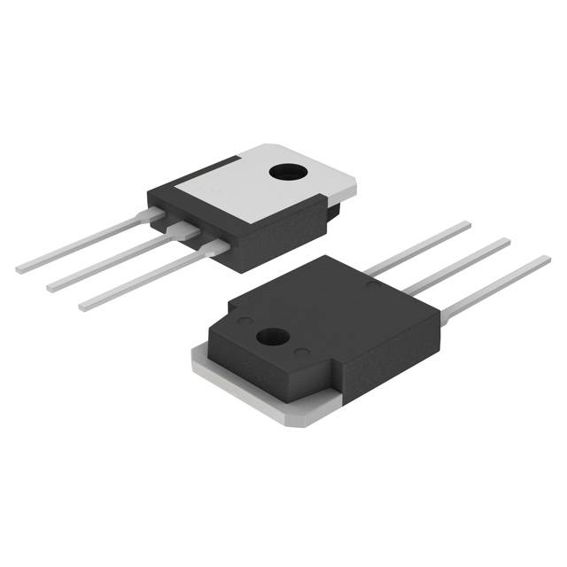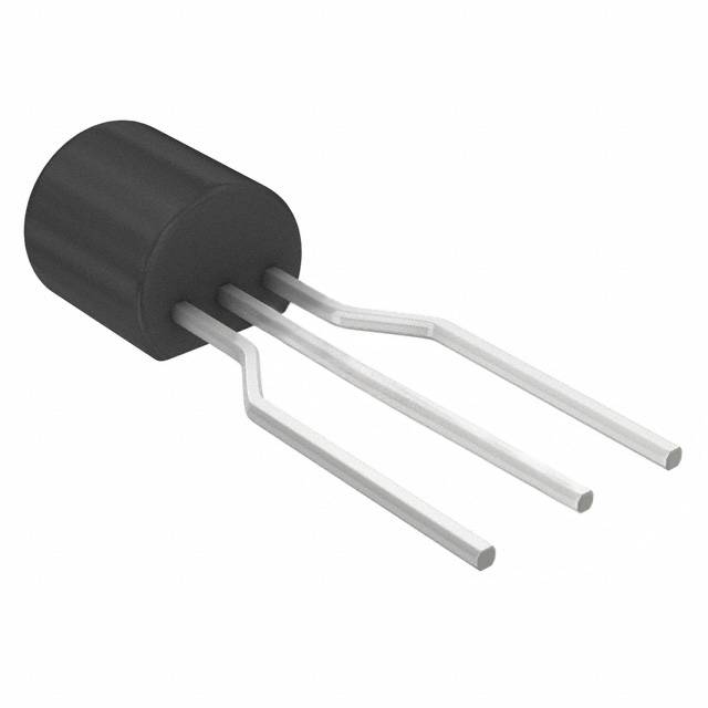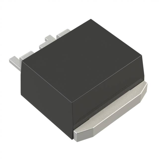
FQA13N50CN-Channel 500 V 13.5A (Tc) 218W (Tc) Through Hole TO-3P
N/A
Orders Over $2000 Receive a $100 Discount for Registered Abrmicro Users.
ABRmicro #.ABR2045-FQA13N-1021305
ManufacturerOnsemi
MPN #.FQA13N50C
Estimated Lead Time-
SampleGet Free Sample
Datasheet FQA13N50C(PDF)
 FQA13N50C(PDF)
For large-volume purchases, our unique channels enable us to provide prices that other suppliers cannot match: significantly below market rates.
Service
 Guaranteed Authenticity
 Technical Support
 Fast Refund
 Free Shipping (over $960)
 Issue an Invoice
 24/7 Manual Service
 Technical Specifications
SeriesQFET®
Packaging
Tube
Lifecycle StatusObsolete
Base Product NumberFQA1
Continuous Drain Current (ID) @ 25°C13.5A (Tc)
Drain-to-Source Voltage (VDS)500 V
Drain-to-Source On Resistance (Max. Min.Rᴅs(on))10V
FET Feature-
FET TypeN-Channel
Gate Charge Total (Qg)(Max.)56 nC @ 10 V
Common Source Input Capacitance (Cɪss)(Max.)@(Vᴅs)2055 pF @ 25 V
Mfronsemi
Mounting StyleThrough Hole
Operating Temperature-55°C ~ 150°C (TJ)
Maximum Power Dissipation218W (Tc)
RDS(on) Drain-to-Source On Resistance480mOhm @ 6.75A, 10V
Package Type (Mfr.)TO-3P
TechnologyMOSFET (Metal Oxide)
Gate-to-Source Voltage (Vɢs)±30V
VGS(th) Gate-to-Source Threshold Voltage (Max.)4V @ 250µA
Package / CaseTO-3P-3, SC-65-3
Customize Part Specifications , or Contact Our Sales Representative to Obtain the Data You Desire info@Abrmicro.com
 info@Abrmicro.com
Extended Links
Datasheets
Environmental Information
PCN Design/Specification
Environmental & Export Classifications
MSL Level1 (Unlimited, ≤ 30°C/85% RH), No special packaging
REACH RegulationNo SVHCs Present
US ECCNEAR99
HTSUS8541.29.0095 (Other; No import duty applies)
Additional Details
The FQA13N50C is a high-voltage N-Channel MOSFET manufactured by Onsemi, designed for efficient power management and switching applications. This component features a drain-source voltage of 500 V and a continuous drain current of 13.5A under controlled conditions (at Tc). It is encapsulated in a TO-3P through-hole package, offering a power dissipation capability of up to 218W (at Tc). The MOSFET exhibits an input capacitance of 2055 pF (at 25 V), a total gate charge of 56 nC (at 10 V), and a gate threshold voltage of 4V (at 250µA), ensuring robust performance in diverse electrical environments.
This information is sourced from the Internet, hasn't been reviewed, and may contain errors.


