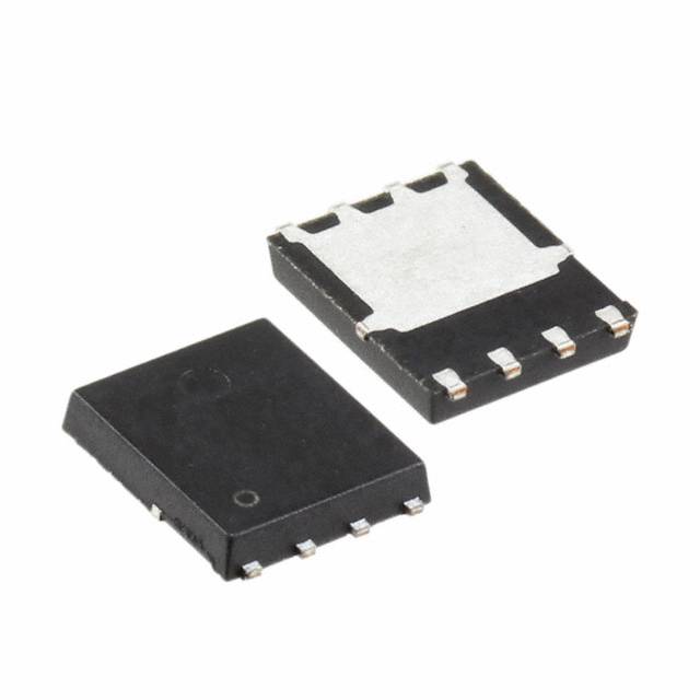
FDWS9509L-F085P-Channel 40 V 65A (Tc) 107W (Tj) Surface Mount 8-DFN (5.1x6.3)
N/A
Orders Over $2000 Receive a $100 Discount for Registered Abrmicro Users.
ABRmicro #.ABR2045-FDWS95-1013343
ManufacturerOnsemi
MPN #.FDWS9509L-F085
Estimated Lead Time-
SampleGet Free Sample
Datasheet FDWS9509L-F085(PDF)
 FDWS9509L-F085(PDF)
For large-volume purchases, our unique channels enable us to provide prices that other suppliers cannot match: significantly below market rates.
Service
 Guaranteed Authenticity
 Technical Support
 Fast Refund
 Free Shipping (over $960)
 Issue an Invoice
 24/7 Manual Service
 Technical Specifications
SeriesPowerTrench®
Packaging
Tape & Reel (TR)
Cut Tape (CT)
Abrmicro® Custom Packaging

Lifecycle StatusObsolete
Base Product NumberFDWS9509
Continuous Drain Current (ID) @ 25°C65A (Tc)
Drain-to-Source Voltage (VDS)40 V
Drain-to-Source On Resistance (Max. Min.Rᴅs(on))4.5V, 10V
FET Feature-
FET TypeP-Channel
Gate Charge Total (Qg)(Max.)67 nC @ 10 V
GradeAutomotive
Common Source Input Capacitance (Cɪss)(Max.)@(Vᴅs)3360 pF @ 20 V
Mfronsemi
Mounting StyleSurface Mount
Operating Temperature-55°C ~ 175°C (TJ)
Maximum Power Dissipation107W (Tj)
QualificationAEC-Q101
RDS(on) Drain-to-Source On Resistance8mOhm @ 65A, 10V
Package Type (Mfr.)8-DFN (5.1x6.3)
TechnologyMOSFET (Metal Oxide)
Gate-to-Source Voltage (Vɢs)±16V
VGS(th) Gate-to-Source Threshold Voltage (Max.)3V @ 250µA
Package / Case8-PowerTDFN
Customize Part Specifications , or Contact Our Sales Representative to Obtain the Data You Desire info@Abrmicro.com
 info@Abrmicro.com
Extended Links
Datasheets
Environmental Information
Forum Discussions
PCN Assembly/Origin
PCN Design/Specification
PCN Obsolescence/ EOL
Environmental & Export Classifications
RoHS ComplianceComplies with RoHS 3 Directive (2015/863/EU)
MSL Level1 (Unlimited, ≤ 30°C/85% RH), No special packaging
REACH RegulationNo SVHCs Present
US ECCNEAR99
HTSUS8541.29.0095 (Other; No import duty applies)
Additional Details
The FDWS9509L-F085 is a P-Channel MOSFET manufactured by Onsemi, designed for surface mounting and housed in an 8-DFN package with dimensions of 5.1x6.3 mm. It is engineered to handle a maximum voltage of 40 V and a continuous current of 65 A under Tc conditions, with a power dissipation of 107 W at Tj. Key characteristics of this component include a gate charge of 67 nC at 10 V, an input capacitance of 3360 pF at 20 V, and a threshold voltage of 3 V at a drain current of 250 µA. This MOSFET is optimized for efficient power management in various electronic applications.
This information is sourced from the Internet, hasn't been reviewed, and may contain errors.


